Electromagnetic interference (EMI) is a significant challenge in today’s electronics, disrupting circuits, degrading signals, and leading to potential malfunctions.
To combat this, PCB shielding plays a pivotal role, offering a reliable solution for minimizing EMI and enhancing device performance.
But what exactly is PCB shielding, and why is it so vital?
PCB shielding uses conductive or magnetic materials to block or reduce EMI, creating a protective barrier around sensitive areas of the printed circuit board.
This ensures clean signals, reliable device operations, and compliance with regulatory standards.
Whether in telecommunications, automotive systems, or medical devices, PCB shielding is indispensable for achieving performance and durability in electronic systems.
In this article, we’ll explore how PCB shielding works, the materials and techniques involved, critical applications, and future trends.
Let’s dive into why PCB shielding is a must-have in modern electronics.
-
Table Of Contents
-
1. Why Is PCB Shielding Crucial for Reliable Electronics?
-
2. How Does PCB Shielding Work to Minimize EMI?
-
3. What Materials and Techniques Are Used in PCB Shielding?
-
4. What Are the Advantages and Challenges of PCB Shielding?
-
5. How Do PCB Shielding and Protection Work Together?
-
6. How Can Simulation Tools Improve PCB Shielding Design?
-
7. How to Ensure Long-Term Shielding Performance?
-
8. What’s Next for PCB Shielding Technology?
-
9. Summary
How Does PCB Shielding Work to Minimize EMI?
At its core, PCB shielding functions through reflection and absorption, blocking or redirecting electromagnetic waves that could interfere with the circuitry.
Here’s how it works:
- Reflection:
- Conductive shields, such as those made from copper or aluminum, create a grounded barrier. This reflects electromagnetic waves away from the circuit, preventing interference.
- Absorption:
- Magnetic materials, like ferrite or specialized alloys, absorb EMI and convert it into harmless heat energy.
To maximize effectiveness, proper shield placement and grounding are critical.
Shields are typically connected to the PCB’s ground plane, redirecting absorbed energy to the ground.
Poor grounding can lead to “ground loops,” which may amplify interference instead of mitigating it.
Common EMI Sources
- External: Radio waves, Wi-Fi routers, or motors.
- Internal: Oscillators, high-speed data lines, or switching power supplies within the PCB itself.
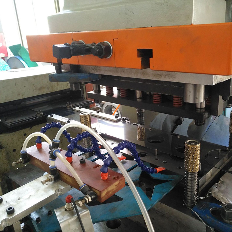
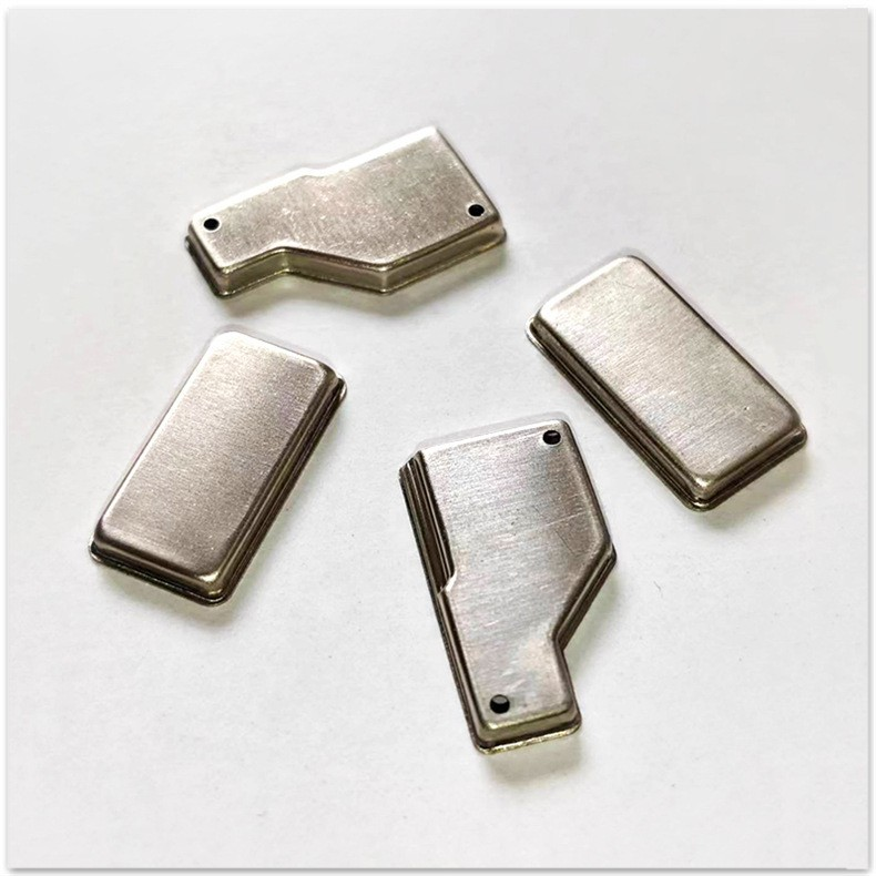
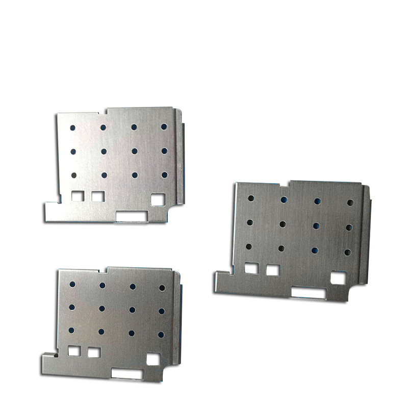
Explore our related metal stamping services that support advanced electronic component manufacturing.
What Materials and Techniques Are Used in PCB Shielding?
Choosing the right materials and techniques is crucial for achieving effective PCB shielding.
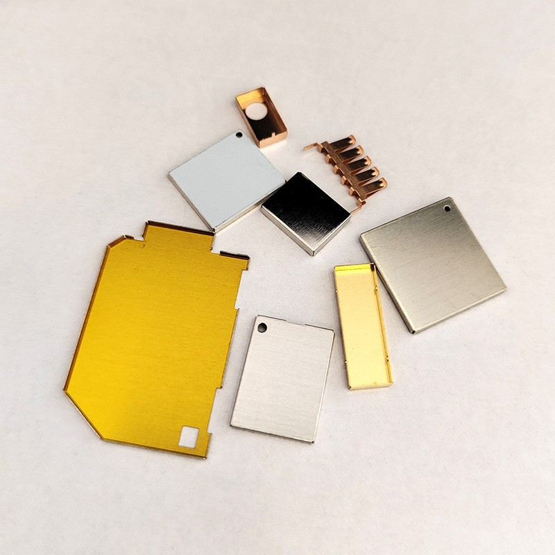
Materials for Shielding
- Conductive Materials:
- Copper: Excellent conductivity and EMI blocking.
- Aluminum: Lightweight and cost-effective.
- Silver: Superior conductivity but expensive.
- Magnetic Materials:
- Ferrite: Ideal for high-frequency EMI.
- Mu-metal: Effective at shielding low-frequency magnetic fields.
- Composite Materials:
- Combine conductive and magnetic properties for hybrid shielding.
Shielding Techniques
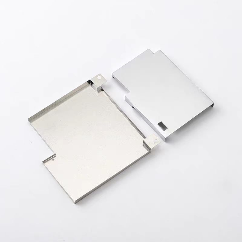
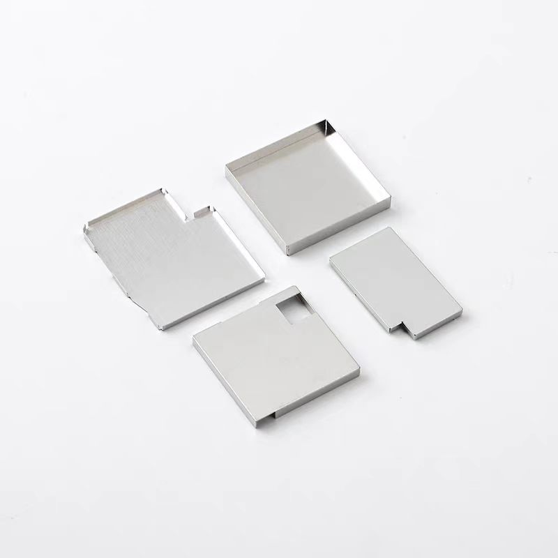
- Metal Enclosures (Cans):
- Robust metallic boxes encasing sensitive components.
- Conductive Coatings:
- Thin layers applied to PCB surfaces or casings.
- EMI Gaskets:
- Flexible seals ensuring a tight shielded enclosure.
- Ground Planes:
- Multi-layer PCBs incorporating dedicated ground planes for added shielding.
What Are the Advantages and Challenges of PCB Shielding?
Benefits of PCB Shielding
- Enhanced Signal Integrity:
- Reduces noise and maintains clean signal transmission.
- Improved Device Reliability:
- Protects components from EMI-induced wear.
- Compliance with Regulations:
- Meets EMI/EMC standards required for market approval.
- Prolonged Product Lifespan:
- Reduces interference-related degradation over time.
Challenges of PCB Shielding
- Design Complexity:
- Requires careful planning and advanced expertise.
- Cost:
- Premium materials and processes can increase expenses.
- Heat Management:
- Shields can trap heat, requiring additional thermal solutions.
- Space Limitations:
- Compact designs must incorporate innovative shielding approaches.
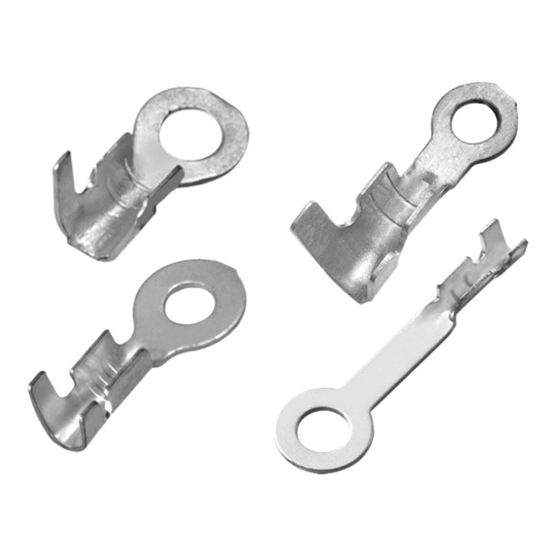
Check out our insights on stamped connectors in challenging environments.
How Do PCB Shielding and Protection Work Together?
While PCB shielding focuses on minimizing EMI, it’s part of a broader strategy for PCB protection:
- Potting:
- Encasing PCBs in protective compounds to shield against vibration, moisture, and EMI.
- Conformal Coatings:
- Transparent layers that guard against dust, corrosion, and interference.
- Thermal Solutions:
- Heat sinks or compounds prevent overheating caused by absorbed EMI.
These complementary techniques ensure optimal performance and longevity for electronic devices.
How Can Simulation Tools Improve PCB Shielding Design?
Simulation tools are revolutionizing the design and optimization of PCB shielding.
These advanced software solutions allow engineers to predict EMI behavior and fine-tune shielding techniques before manufacturing.
- Accurate EMI Analysis:
- Simulation tools provide detailed insights into potential EMI sources and their impact on the PCB. This helps in identifying vulnerable areas that require shielding.
- Optimized Shield Placement:
- By visualizing electromagnetic fields, engineers can strategically position shields to maximize effectiveness without adding unnecessary materials or weight.
- Cost and Time Efficiency:
- Testing different shielding designs in a virtual environment reduces the need for physical prototypes, cutting both development costs and lead times.
- Integration with Thermal Management:
- Simulation tools can analyze heat dissipation in conjunction with EMI shielding, ensuring that thermal and electromagnetic considerations are balanced.
By leveraging simulation tools, designers can create PCB shielding solutions that are efficient, cost-effective, and tailored to the unique demands of each application.
How to Ensure Long-Term Shielding Performance?
To maintain effective shielding over time, proper maintenance and strategic practices are essential:
- Regular Inspections:
- Check for wear or corrosion that could compromise shielding.
- Thermal Management:
- Use vents or heat-resistant materials to prevent overheating.
- Environmental Protection:
- Ensure shields are sealed against moisture and contaminants.
- Material Upgrades:
- Consider replacing outdated shields with advanced materials for better performance.
By implementing these steps, you can maximize the effectiveness and lifespan of PCB shielding solutions.
What’s Next for PCB Shielding Technology?
As technology evolves, so do PCB shielding methods:
- Advanced Materials:
- Lightweight, eco-friendly shielding materials are emerging.
- Integrated Shielding:
- Embedding shielding directly into PCB layers for compact designs.
- 3D Printing:
- Custom-fit shields created through 3D printing for precision applications.
- Automation:
- Streamlining shielding application during manufacturing for cost efficiency.
These innovations promise enhanced performance and adaptability for future electronic designs.
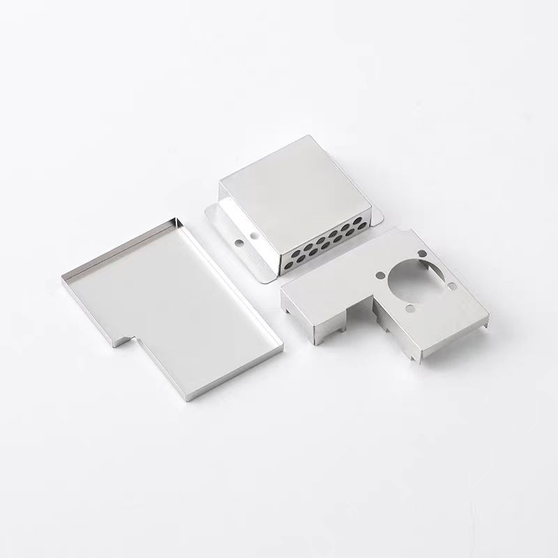
Learn more about our metal stamping parts for consumer electronics.
Conclusion
PCB shielding is an indispensable solution for mitigating EMI and ensuring the reliable performance of modern electronics.
Blocking unwanted interference enhances signal integrity, improves device reliability, and ensures compliance with regulatory standards.
From telecommunications to medical devices, the benefits of PCB shielding are evident across industries.
While challenges like heat management and cost exist, advancements in materials and techniques pave the way for more efficient solutions.